
SY110-SIP
Functional description
Overview
Revolutionized New Platform for All Integrated Smart & Secure Sensors
Next generation applications in logistics, robotics, automation, smart home and building, consumer and white goods, smart city and renewable energy require the adaption of smart and secure sensors with data connectivity. Existing semiconductor standard solutions often provide insufficient flexibility and missing software environment. The most critical item, however, is the missing inherent data security approach encompassing the complete value chain of the product.
The Solution
Sensry is a newly established company offers an smart edge sensor construction kit with highly flexible and customizable hardware configurations according to customer requirements. The universal sensor platform USeP combines cutting-edge assembly and packaging technologies with new design methods as well as various integration possibilities for sensors.
Features
- Integration of various sensors on Package Top Level
- Support of multiple communication standards
- Low power consumption
- Multi-Core RISC-V performance for smart edge computing
- Adequate memory resources
- Inherent multi-layer data security and authentication
- Fast design using standard library HW components
- Smallest form factor due to advanced 3D-packaging
- SDK & Toolchain available
- Integration in fog, edge and cloud computing
- Optional integration support from Sensry
Key Features
- Sensor Integration on Package Top-Level
- Acceleration
- Gyroskope
- Magnetometer
- Vibration
- Temperature
- Pressure
- Humidity
- VOC
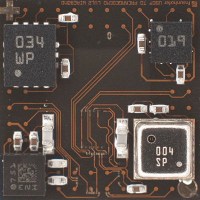
Package Top Level
The 3D-System-in-Package provides numerous interfaces to the Top- and Bottom-Level.
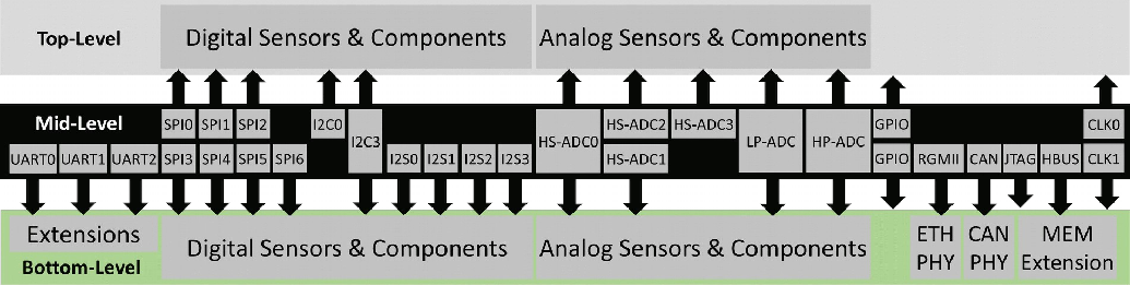
The system has digital and analog interfaces to connect sensor devices to the system. There are three different Analog-to-Digital converters integrated. Two complex wired interfaces are supported by the Ganymed® core: Ethernet TSN and CAN-FD. These communication interfaces require an external physical layer. All interfaces are described in separate sections.
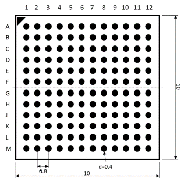
The Bottom-Level is the interface to the embedded customer system in form of a BGA-144 footprint with a pitch of 0.8mm and a ball diameter of 0.4mm. Please refer to section to find the footprint dimensions. The interface distribution is divided into several power and management pins and the I/ O interface. Figure 4 shows the general pin out of the device from top view
The Top-Level is the interface to the Package-on-Package sensor or peripheral parts. The application specific sensors are assembled on top side of the sensor PCB. The bottom side of the sensor PCB is the interface to the Ganymed® system. The interface includes power sources and different digital and analog interfaces. The Top-Level Figure 5 illustrates the different available interfaces.
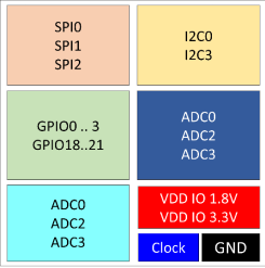
| Block | Signal | Voltage | Note |
|---|---|---|---|
| SPI0 | SCK | 1.8 V | System Clock |
| SPI0 | SDO | 1.8 V | Data Out |
| SPI0 | SDI | 1.8 V | Data In |
| SPI0 | nCS0 | 1.8 V | Chip Select 0 (low active) |
| SPI0 | nCS1 | 1.8 V | Chip Select 1 (low active) |
| SPI1 | SCK | 1.8 V | System Clock |
| SPI1 | SDO | 1.8 V | Data Out |
| SPI1 | SDI | 1.8 V | Data In |
| SPI1 | nCS0 | 1.8 V | Chip Select 0 (low active) |
| SPI1 | nCS1 | 1.8 V | Chip Select 1 (low active) |
| SPI2 | SCK | 1.8 V | System Clock |
| SPI2 | SDO | 1.8 V | Data Out |
| SPI2 | SDI | 1.8 V | Data In |
| SPI2 | nCS0 | 1.8 V | Chip Select 0 (low active) |
| SPI2 | nCS1 | 1.8 V | Chip Select 1 (low active) |
| I2C0 | SCL | 1.8 V | Clock |
| I2C0 | SDA | 1.8 V | Data |
| I2C3 | SCL | 1.8 V | Clock - I2C3 is additionally available on Bottom Level |
| I2C3 | SDA | 1.8 V | Data - I2C3 is additionally available on Bottom Level |
| GPIO | 0 | 1.8 V | |
| GPIO | 1 | 1.8 V | |
| GPIO | 2 | 1.8 V | |
| GPIO | 3 | 1.8 V | |
| GPIO | 18 | 1.8 V | |
| GPIO | 19 | 1.8 V | |
| GPIO | 20 | 1.8 V | |
| GPIO | 21 | 1.8 V | |
| ADC0 | VIN_P | Analog | Parallel HS-ADC0-VIN_P, LP-ADC-VIN_P, HP-ADC-VIN_P |
| ADC0 | VIN_N | Analog | Parallel HS-ADC0-VIN_N, LP-ADC-VIN_N, HP-ADC-VIN_N |
| ADC2 | VIN_P | Analog | High Speed ADC2-VIN_P |
| ADC2 | VIN_N | Analog | High Speed ADC2-VIN_N |
| ADC3 | VIN_P | Analog | High Speed ADC3-VIN_P |
| ADC3 | VIN_N | Analog | High Speed ADC3-VIN_N |
| CLOCK | CLOCK0 | 25MHz Main clock oscillator input | |
| VDD IO | 3.3V | 3.3V Supply for sensors and peripherals | |
| VDD IO | 1.8V | 1.8V Supply for sensors and peripherals | |
| VSS IO | GND | GND for sensors and peripherals |
All the described signals and power supplies can be access on the top level. The main clock oscillator is mandatory on the top level. Any kind of digital or analog sensors which fits onto the size of the chip can be assembled on the Package Top-Level.
Sensors
The system is considered as an adaptable system in package (3D-SiP) and split into a costumer specific Embedded System Layer (Bottom-Level), a fixed Processing Layer (Mid-Level) and a costumer specific variable Sensor Layer (Top-Level). The interface assembly layer connecting Top- and Mid-Level is customizable and can be equipped with a variety of different sensors. The footprint of the chip to the costumer specific system is fixed.

Top Level: The Sensor Area
Top of the processing layer additional sensors and devices can be assembled package-on-package. Referring to Figure 5 a subset of communication interfaces is available to connect a variety of sensors. The footprint is an outlined ball grid array with access to the power sources and analog and digital interface to connect the devices. The type of sensor will be defined and placed by costumer based on the set of selectable devices. The complete system in package will be manufactured in the SENSRY supply chain in order to get a costumer specific device.
The sensors can be selected by costumer. A standard sensor implementation is available:
| Sensor class | Sensor type | Manufacturer | Sensor name |
|---|---|---|---|
| Environment | Humidity | Bosch Sensortec | BME680 |
| Environment | Temperature | Bosch Sensortec | BME680 |
| Environment | Air pressure | Bosch Sensortec | BME680 |
| Gas | bVOC | Bosch Sensortec | BME680 |
| Gas | CO2 | Bosch Sensortec | BME680 |
| Intertial | Acceleration | Bosch Sensortec | BMA456 |
| Intertial | Vibration | STMicroelectronics | MIS2DH |
| Inertial | Angular rate | Bosch Sensortec | BMG250 |
Example Top-Level assembly
The following table describes a possible variant of sensor sizes on Top-Level.
| Device | Measured value | Man. | Size [mm] | Interface | Pack |
|---|---|---|---|---|---|
| BME680 | Temperature, Pressure, Humidity, VOC | Bosch | 3.0 x 3.0 x 0.93 | SPI | LGA |
| BMA456 | Acceleration (3-axis) | Bosch | 2.0 x 2.0 x 0.65 | SPI | LGA |
| MIS2DH | Vibraton | ST Micro | 2.0 x 2.0 x 1.0 | I2C | LGA |
| BMG250 | Gyroscope (3-axis) | Bosch | 2.5 x 3.0 x 0.83 | SPI | LGA |
Pin description
The Bottom-Level consists of the costumer specific PCB design. The System-in-Package will be placed and routed as a normal electronic part. The PCB represents the costumer specific geometric constraints, needed passives and power regulation and additional devices like memory, sensors and RF-bridges. The contract point between Bottom-Level and Mid-Level is the bottom footprint of the system in package which is defined as a standard ball grid array with a pitch of 0.8mm.
The costumer is free to adapted additional sensors, devices o RF-capabilities on the PCB of the Embedded System. Fort a certain number of sensors there will be an integration support by Sensry. This includes the integration in the software application programming interface (Sensor-API).
| Pad | Block | Signal | Voltage | Note |
|---|---|---|---|---|
| A2 | UART0 | TX | 1.8 V | Transmit |
| A1 | UART0 | RX | 1.8 V | Receive |
| A7 | UART1 | TX | 3.3 V | Transmit |
| A6 | UART1 | RX | 3.3 V | Receive |
| B6 | UART1 | RTS | 3.3 V | Ready to Send |
| C6 | UART1 | CTS | 3.3 V | Clear to Send |
| C8 | UART2 | TX | 3.3 V | Transmit |
| B8 | UART2 | RX | 3.3 V | Receive |
| C7 | UART2 | RTS | 3.3 V | Ready to Send |
| B7 | UART2 | CTS | 3.3 V | Clear to Send |
| A10 | SPI3 | SCK | 3.3 V | System Clock |
| B10 | SPI3 | SDO | 3.3 V | Data Out |
| A11 | SPI3 | SDI | 3.3 V | Data In |
| B11 | SPI3 | nCS0 | 3.3 V | Chip Select 0 (low active) |
| A12 | SPI3 | nCS1 | 3.3 V | Chip Select 1 (low active) |
| C10 | SPI4 | SCK | 3.3 V | System Clock |
| B12 | SPI4 | SDO | 3.3 V | Data Out |
| D10 | SPI4 | SDI | 3.3 V | Data In |
| C11 | SPI4 | nCS0 | 3.3 V | Chip Select 0 (low active) |
| C12 | SPI4 | nCS1 | 3.3 V | Chip Select 1 (low active) |
| E10 | SPI5 | SCK | 3.3 V | System Clock |
| D11 | SPI5 | SDO | 3.3 V | Data Out |
| D12 | SPI5 | SDI | 3.3 V | Data In |
| E11 | SPI5 | nCS0 | 3.3 V | Chip Select 0 (low active) |
| E12 | SPI5 | nCS1 | 3.3 V | Chip Select 1 (low active) |
| F10 | SPI6 | SCK | 3.3 V | System Clock |
| F12 | SPI6 | SDO | 3.3 V | Data Out |
| G12 | SPI6 | SDI | 3.3 V | Data In |
| F11 | SPI6 | nCS0 | 3.3 V | Chip Select 0 (low active) |
| G10 | SPI6 | nCS1 | 3.3 V | Chip Select 1 (low active) |
| C9 | I2C1 | SCL | 3.3 V | Clock |
| B9 | I2C1 | SDA | 3.3 V | Data |
| A9 | I2C2 | SCL | 3.3 V | Clock |
| A8 | I2C2 | SDA | 3.3 V | Data |
| D1 | I2C3 | SCL | 3.3 V | Clock - I2C3 is additionally available on Sensor Level |
| E1 | I2C3 | SDA | 3.3 V | Data - I2C3 is additionally available on Sensor Level |
| L8 | GPIO | 4 | 3.3 V | General Purpose I/O and PWM |
| K8 | GPIO | 5 | 3.3 V | General Purpose I/O and PWM |
| M7 | GPIO | 6 | 3.3 V | General Purpose I/O and PWM |
| M6 | GPIO | 7 | 3.3 V | General Purpose I/O and PWM |
| K9 | GPIO | 8 | 3.3 V | General Purpose I/O and PWM |
| L9 | GPIO | 9 | 3.3 V | General Purpose I/O and PWM |
| M9 | GPIO | 10 | 3.3 V | General Purpose I/O and PWM |
| M8 | GPIO | 11 | 3.3 V | General Purpose I/O and PWM |
| L12 | GPIO | 12 | 3.3 V | General Purpose I/O and PWM |
| M12 | GPIO | 13 | 3.3 V | General Purpose I/O and PWM |
| M11 | GPIO | 14 | 3.3 V | General Purpose I/O and PWM |
| M10 | GPIO | 15 | 3.3 V | General Purpose I/O and PWM |
| M5 | GPIO | 16 | 1.8 V | General Purpose I/O and PWM |
| M4 | GPIO | 17 | 1.8 V | General Purpose I/O and PWM |
| C5 | RGMII1 | TXC | 1.8 V | Reduced Gigabit Media Independent Interface |
| B4 | RGMII1 | TXD0 | 1.8 V | Reduced Gigabit Media Independent Interface |
| A4 | RGMII1 | TXD1 | 1.8 V | Reduced Gigabit Media Independent Interface |
| A5 | RGMII1 | TXD2 | 1.8 V | Reduced Gigabit Media Independent Interface |
| B5 | RGMII1 | TXD3 | 1.8 V | Reduced Gigabit Media Independent Interface |
| A3 | RGMII1 | TX_CTL | 1.8 V | Reduced Gigabit Media Independent Interface |
| C4 | RGMII1 | RXC | 1.8 V | Reduced Gigabit Media Independent Interface |
| C2 | RGMII1 | RXD0 | 1.8 V | Reduced Gigabit Media Independent Interface |
| C3 | RGMII1 | RXD1 | 1.8 V | Reduced Gigabit Media Independent Interface |
| B2 | RGMII1 | RXD2 | 1.8 V | Reduced Gigabit Media Independent Interface |
| B3 | RGMII1 | RXD3 | 1.8 V | Reduced Gigabit Media Independent Interface |
| E4 | RGMII1 | RX_CTL | 1.8 V | Reduced Gigabit Media Independent Interface |
| B1 | RGMII1 | MDC | 1.8 V | Reduced Gigabit Media Independent Interface |
| C1 | RGMII1 | MDIO | 1.8 V | Reduced Gigabit Media Independent Interface |
| F4 | CAN | IN | 1.8 V | Controller Area Network Interface |
| F5 | CAN | OUT | 1.8 V | Controller Area Network Interface |
| F6 | CAN | SHDN | 1.8 V | Controller Area Network Interface |
| L3 | JTAG0 | TDI | 3.3 V | Debug JTAG |
| K3 | JTAG0 | TDO | 3.3 V | Debug JTAG |
| M2 | JTAG0 | TCK | 3.3 V | Debug JTAG |
| L2 | JTAG0 | TMS | 3.3 V | Debug JTAG |
| K2 | JTAG0 | TRST | 3.3 V | Debug JTAG |
| M3 | JTAG1 | TDI | 3.3 V | System-Test JTAG |
| L4 | JTAG1 | TDO | 3.3 V | System-Test JTAG |
| K4 | JTAG1 | TCK | 3.3 V | System-Test JTAG |
| L5 | JTAG1 | TMS | 3.3 V | System-Test JTAG |
| K5 | JTAG1 | TRST | 3.3 V | System-Test JTAG |
| K10 | I2S0 | SCK | 3.3 V | Bit Clock |
| J10 | I2S0 | SWS | 3.3 V | Left/Right Clock |
| H10 | I2S0 | SDI | 3.3 V | Data |
| K11 | I2S1 | SCK | 3.3 V | Bit Clock |
| L11 | I2S1 | SWS | 3.3 V | Left/Right Clock |
| L10 | I2S1 | SDI | 3.3 V | Data |
| G11 | I2S2 | SCK | 3.3 V | Bit Clock |
| H11 | I2S2 | SWS | 3.3 V | Left/Right Clock |
| J11 | I2S2 | SDI | 3.3 V | Data |
| H12 | I2S3 | SCK | 3.3 V | Bit Clock |
| J12 | I2S3 | SWS | 3.3 V | Left/Right Clock |
| K12 | I2S3 | SDI | 3.3 V | Data |
| K7 | ADC0 | VIN_P | analog | Parallel HS-ADC0-VIN_P, LP-ADC-VIN_P, HP-ADC-VIN_P |
| L7 | ADC0 | VIN_N | analog | Parallel HS-ADC0-VIN_N, LP-ADC-VIN_N, HP-ADC-VIN_N |
| L6 | ADC1 | VIN_P | analog | |
| K6 | ADC1 | VIN_N | analog | |
| J1 | HYPERBUS | CS1 | 1.8 V | |
| H2 | HYPERBUS | CS2 | 1.8 V | |
| E3 | HYPERBUS | CLK_P | 1.8 V | |
| D3 | HYPERBUS | CLK_N | 1.8 V | |
| H1 | HYPERBUS | RWDS | 1.8 V | |
| G3 | HYPERBUS | DQ0 | 1.8 V | |
| G2 | HYPERBUS | DQ1 | 1.8 V | |
| G1 | HYPERBUS | DQ2 | 1.8 V | |
| F2 | HYPERBUS | DQ3 | 1.8 V | |
| F1 | HYPERBUS | DQ4 | 1.8 V | |
| E2 | HYPERBUS | DQ5 | 1.8 V | |
| D2 | HYPERBUS | DQ6 | 1.8 V | |
| F3 | HYPERBUS | DQ7 | 1.8 V | |
| K1 | RESET | 3.3 V | System Reset (Low Active) | |
| H3 | CLOCK1 | 3.3V | 32.768kHz oscillator input | |
| D9 | VDD IO | 1.8 V | I/O Supply | |
| D4 | VDD IO | 1.8 V | ||
| G9 | VDD IO | 1.8 V | ||
| J9 | VDD IO | 1.8 V | ||
| H4 | VDD IO | 1.8 V | MRAM | |
| E9 | VDD IO | 3.3 V | ||
| G5 | VDD IO | 3.3 V | ||
| D8 | VDD CORE | 0.8V | Core Supply | |
| E7 | VDD CORE | 0.8V | ||
| F8 | VDD CORE | 0.8V | ||
| G7 | VDD CORE | 0.8V | ||
| H8 | VDD CORE | 0.8V | ||
| H7 | VDD ANALOG | 1.8V | Analog Sub-System Supply | |
| J7 | VDD ANALOG | 1.8V | ||
| H5 | VDD MRAM | 1.8V | MRAM Supply | |
| J5 | VDD MRAM | 0.8V | MRAM Supply | |
| J4 | VREF MRAM | 0.6V | MRAM Reference Voltage (must set to 0.6V) | |
| J4 | VSS CORE | GND | CORE Ground | |
| F7 | VSS CORE | GND | ||
| G8 | VSS CORE | GND | ||
| G6 | VSS CORE | GND | ||
| H6 | VSS CORE | GND | ||
| D7 | VSS IO | GND | IO Ground | |
| F9 | VSS IO | GND | ||
| H9 | VSS IO | GND | ||
| J8 | VSS IO | GND | ||
| D6 | VSS BIAS DPU | GND | DPU Bias Ground | |
| G4 | VSS MRAM | GND | MRAM Ground | |
| J6 | VSS ANALOG | GND | Analog Ground | |
| E6 | BIAS DPU | 1.8V | DPU BIAS Voltage (must set to fixed 1.8V) | |
| D5 | BIAS DPU | GND | DPU BIAS Ground | |
| E5 | BIAS DPU | GND | DPU BIAS Ground | |
| M1 | BOOT MODE | BOOTM0 | 3.3 V | Bootloader settings |
| L1 | BOOT MODE | BOOTM1 | 3.3 V | Bootloader settings |
| J2 | TEST | TEST MODE | 1.8 V | Set fix to 1.8V |
| J3 | TEST | SCAN ENABLE | 1.8 V | Set fix to 1.8V |
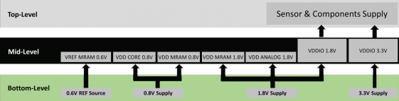
Power
| Core Voltage | 0.8V |
| IO voltage | 1.8V and 3.3V |
| MRAM voltage reference | 0.6V |
| Analog Subsystem voltages | 0.8V and 1.8V |
| Maximum total power dissipation | < 1W |
Three different power domains and one reference voltage are required for the Ganymed® system. On Top-Level the IO voltages are available to supply the sensors and peripherals.
Clocks
| Low power operation clock/boot clock | 32.768kHz |
| System reference clock(external oscillator) | 25MHz |
The CPU clock frequency can be set exclusively by the DAQU CPU core. All DPU cores operate at the same clock frequency (unless disabled), while the DAQU core frequency may be different.
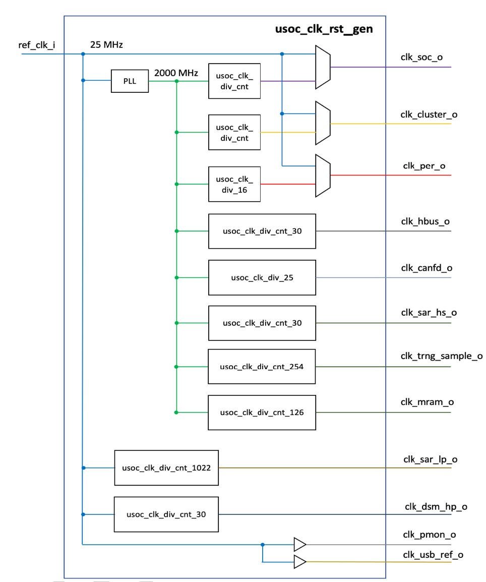
All the internal clocks are derived from a single PLL operating at a VCO clock source of 2 GHz generated from an extern reference clock of 25MHz. Most of the internal clock dividers are configurable. The DAQU and the peripheral logic can be multiplexed into the 25MHz reference clock domain to provide basic functionality if the PLL and clock dividers are uninitialized.