
SY120-GBM
Functional description
Overview
Revolutionized New Platform for All Integrated Smart & Secure Sensors
Next generation applications in logistics, robotics, automation, smart home and building, consumer and white goods, smart city and renewable energy require the adaption of smart and secure sensors with data connectivity. Existing semiconductor standard solutions often provide insufficient flexibility and missing software environment. The most critical item, however, is the missing inherent data security approach encompassing the complete value chain of the product.
The Solution
Sensry is a newly established company offers an smart edge sensor construction kit with highly flexible and customizable hardware configurations according to customer requirements. The universal sensor platform USeP combines cutting-edge assembly and packaging technologies with new design methods as well as various integration possibilities for sensors.
Features of the Generic Base Module (GBM)
- Top level interface for extension PCB (i.e. sensors)
- Support of multiple communication standards
- Low power consumption
- Multi-Core RISC-V performance for smart edge computing
- Adequate memory resources
- Inherent multi-layer data security and authentication
- Fast design using standard library HW components
- Smallest form factor due to advanced 3D-packaging
- SDK & Toolchain available
- Integration in fog, edge and cloud computing
- Optional integration support from Sensry
Key Features
- Processing Unit
- RISC-V based cluster core (max. 400MHz)
- 1 RISCY Data acquisition Unit (DAQU)
- 8 RISCY Data Proc. Units (DPU) with FPU
- Event bus
- DMA
- Security features
- Crypto Co-Processor
- Secure Boot ROM
- Secure MRAM / SRAM
- True Random Number Generator (TRNG)
- One-Time-Programmable Memory (OTP) for Keys and Certificates
- Interfaces
- 3x UART (up to 2Mbit/s, two of them with hardware handshake)
- 4x I2C (up to 400kHz)
- 4x I2S
- 7x SPI (up to 50MHz)
- CAN-FD
- RGMII with MDIO for Ethernet-Phy
- HyperBus (for external RAM/Flash)
- Debug JTAG
- 25MS/s 12bit SAR ADC
- 100kS/s 11bit ultra low power SAR ADC
- 16Bit Sigma Delta ADC (Audio)
- 32 GPIO (configurable for 1.8V or 3.3V operation)
- Each interface (except GPIO) can be induvidually disabled for power saving
- Memory
- 512kB Secure MRAM
- 512kB MRAM
- 4MB SRAM
- Individual Data & Instruction Cache for the DPU
Interfaces
The 3D-System-in-Package provides numerous interfaces to the Top- and Bottom-Level.
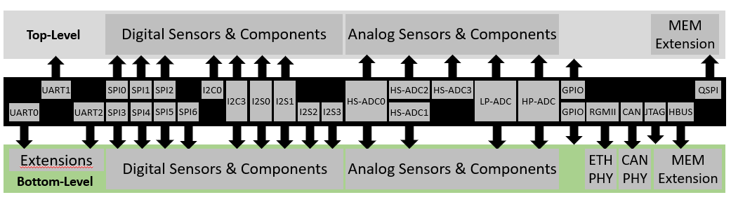
The system has digital and analog interfaces to connect sensor devices to the system. There are three different Analog-to-Digital converters integrated. Two complex wired interfaces are supported by the Ganymed® core: Ethernet TSN and CAN-FD. These communication interfaces require an external physical layer. All interfaces are described in separate sections.
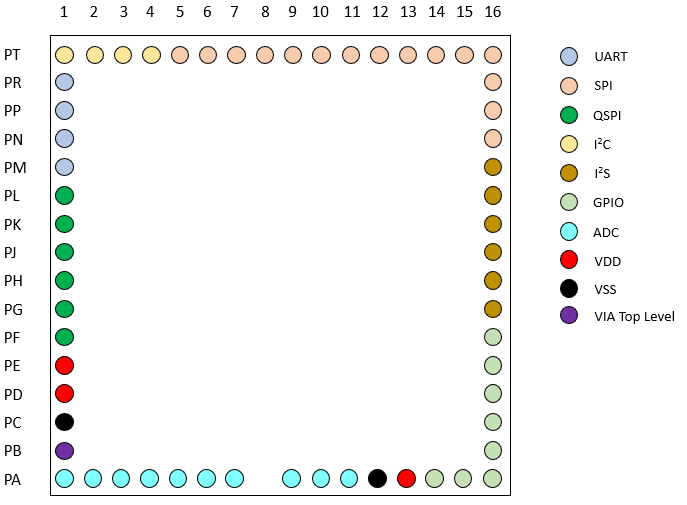
The Bottom-Level is the interface to the embedded customer system in form of a BGA-144 footprint with a pitch of 0.8mm and a ball diameter of 0.4mm. Please refer to section to find the footprint dimensions. The interface distribution is divided into several power and management pins and the I/ O interface. Figure 4 shows the general pin out of the device from top view
The Top-Level is the interface to the Package-on-Package sensor or peripheral parts. The application specific sensors are assembled on top side of the sensor PCB. The bottom side of the sensor PCB is the interface to the Ganymed® system. The interface includes power sources and different digital and analog interfaces. The Top-Level Figure 5 illustrates the different available interfaces.
Pin definitions
Top Level Footprint
| Pad | Block | Signal | Voltage | Note |
|---|---|---|---|---|
| PT7 | SPI0 | SCK | 1.8 V | System Clock |
| PT6 | SPI0 | SDO | 1.8 V | Data Out |
| PT5 | SPI0 | SDI | 1.8 V | Data In |
| PT9 | SPI0 | nCS0 | 1.8 V | Chip Select 0 (low active) |
| PT8 | SPI0 | nCS1 | 1.8 V | Chip Select 1 (low active) |
| PT12 | SPI1 | SCK | 1.8 V | System Clock |
| PT11 | SPI1 | SDO | 1.8 V | Data Out |
| PT10 | SPI1 | SDI | 1.8 V | Data In |
| PT14 | SPI1 | nCS0 | 1.8 V | Chip Select 0 (low active) |
| PT13 | SPI1 | nCS1 | 1.8 V | Chip Select 1 (low active) |
| PR16 | SPI2 | SCK | 1.8 V | System Clock |
| PT16 | SPI2 | SDO | 1.8 V | Data Out |
| PT15 | SPI2 | SDI | 1.8 V | Data In |
| PN16 | SPI2 | nCS0 | 1.8 V | Chip Select 0 (low active) |
| PP16 | SPI2 | nCS1 | 1.8 V | Chip Select 1 (low active) |
| PK1 | QSPI | SCK | 1.8 V | System Clock |
| PJ1 | QSPI | SDIO0 | 1.8 V | Data0 |
| PH1 | QSPI | SDIO1 | 1.8 V | Data1 |
| PG1 | QSPI | SDIO2 | 1.8 V | Data2 |
| PF1 | QSPI | SDIO3 | 1.8 V | Data3 |
| PL1 | QSPI | CS | 1.8 V | Chip Select |
| PT4 | I2C0 | SCL | 1.8 V | Clock |
| PT3 | I2C0 | SDA | 1.8 V | Data |
| PT2 | I2C3 | SCL | 1.8 V | Clock |
| PT1 | I2C3 | SDA | 1.8 V | Data |
| PH16 | I2S0 | SCK | 1.8 V | Clock |
| PG16 | I2S0 | SDI | 1.8 V | Data In |
| PJ16 | I2S0 | SWS | 1.8 V | Word Select |
| PL16 | I2S1 | SCK | 1.8 V | Clock |
| PK16 | I2S1 | SDI | 1.8 V | Data In |
| PM16 | I2S1 | SWS | 1.8 V | Word Select |
| PR1 | UART1 | RX | 1.8 V | Receive |
| PP1 | UART1 | RX | 1.8 V | Receive |
| PN1 | UART1 | RTS | 1.8 V | Ready to Send |
| PM1 | UART1 | CTS | 1.8 V | Clear to Send |
| PF16 | GPIO | 0 | 1.8 V | |
| PE16 | GPIO | 1 | 1.8 V | |
| PD16 | GPIO | 2 | 1.8 V | |
| PC16 | GPIO | 3 | 1.8 V | |
| PB16 | GPIO | 18 | 1.8 V | |
| PA16 | GPIO | 19 | 1.8 V | |
| PA15 | GPIO | 20 | 1.8 V | |
| PA14 | GPIO | 21 | 1.8 V | |
| PA5 | HS-ADC0 | VIN_P | Analog | High Speed ADC VIN_P 0 |
| PA4 | HS-ADC0 | VIN_N | Analog | High Speed ADC VIN_N 0 |
| PA2 | HS-ADC1 | VIN_P | Analog | High Speed ADC VIN_P 1 |
| PA1 | HS-ADC1 | VIN_N | Analog | High Speed ADC VIN_N 1 |
| PA10 | LP-ADC | VIN_P | Analog | Low Power ADC VIN_P |
| PA11 | LP-ADC | VIN_N | Analog | Low Power ADC VIN_N |
| PA6 | HP-ADC | VIN_P | Analog | High Precision ADC VIN_P |
| PA3 | HP-ADC | VIN_N | Analog | High Precision ADC VIN_N |
| PA7 | RES | Reserved | Analog | Reserved Pin |
| PA9 | RES | Reserved | Analog | Reserved Pin |
| PD1 | VDD IO | 3.3V | 3.3V Supply | |
| PE1 | VDD IO | 1.8V | 1.8V Supply | |
| PC1 | VSS IO | GND | Digital GND | |
| PA13 | VDDA | 1.8V | 1.8V Analog Supply | |
| PA12 | VSSA | GND | Analog GND | |
| PB1 | Spare Through | Spare Through between PCB and Package Top Level |
All the described signals and power supplies can be access on the top level. Any kind of digital or analog component which fits onto the size of the chip can be assembled on the Package Top-Level PCB.
Bottom Level Footprint

Notes:
- Additional physical layer is needed to use the CAN or Ethernet TSN (RGMII) interface
- The ADC0 and ADC4 interfaces are parallel connected High-Speed-ADC, Low-Power-ADC and High-Precision-ADC input:
- ADC0-VIN_P = HS-ADC0-VIN_P = LP-ADC-VIN_P = HP-ADC-VIN_P
- ADC0-VIN_N = HS-ADC0-VIN_N = LP-ADC-VIN_N = HP-ADC-VIN_N
| Pad | Block | Signal | Voltage | Note |
|---|---|---|---|---|
| K6 | UART0 | TX | 1.8 V | Transmit |
| L6 | UART0 | RX | 1.8 V | Receive |
| N7 | UART2 | TX | 3.3 V | Transmit |
| L7 | UART2 | RX | 3.3 V | Receive |
| M7 | UART2 | RTS | 3.3 V | Ready to Send |
| H8 | UART2 | CTS | 3.3 V | Clear to Send |
| N11 | SPI3 | SCK | 1.8 V | System Clock |
| M9 | SPI3 | SDO | 1.8 V | Data Out |
| L9 | SPI3 | SDI | 1.8 V | Data In |
| M10 | SPI3 | nCS0 | 1.8 V | Chip Select 0 (low active) |
| L10 | SPI3 | nCS1 | 1.8 V | Chip Select 1 (low active) |
| M11 | SPI4 | SCK | 1.8 V | System Clock |
| N13 | SPI4 | SDO | 1.8 V | Data Out |
| M12 | SPI4 | SDI | 1.8 V | Data In |
| N12 | SPI4 | nCS0 | 1.8 V | Chip Select 0 (low active) |
| L12 | SPI4 | nCS1 | 1.8 V | Chip Select 1 (low active) |
| M13 | SPI5 | SCK | 3.3 V | System Clock |
| L11 | SPI5 | SDO | 3.3 V | Data Out |
| K10 | SPI5 | SDI | 3.3 V | Data In |
| L13 | SPI5 | nCS0 | 3.3 V | Chip Select 0 (low active) |
| F8 | SPI5 | nCS1 | 3.3 V | Chip Select 1 (low active) |
| K11 | SPI6 | SCK | 3.3 V | System Clock |
| J10 | SPI6 | SDO | 3.3 V | Data Out |
| D7 | SPI6 | SDI | 3.3 V | Data In |
| E7 | SPI6 | nCS0 | 3.3 V | Chip Select 0 (low active) |
| J12 | SPI6 | nCS1 | 3.3 V | Chip Select 1 (low active) |
| N10 | I2C1 | SCL | 1.8 V | Clock |
| K8 | I2C1 | SDA | 1.8 V | Data |
| N9 | I2C2 | SCL | 3.3 V | Clock |
| L8 | I2C2 | SDA | 3.3 V | Data |
| N8 | I2C3 | SCL | 1.8 V | Clock - I2C3 is additionally available on Sensor Level |
| M8 | I2C3 | SDA | 1.8 V | Data - I2C3 is additionally available on Sensor Level |
| A11 | GPIO | 4 | 1.8 V | General Purpose I/O and PWM |
| C11 | GPIO | 5 | 1.8 V | General Purpose I/O and PWM |
| A13 | GPIO | 6 | 1.8 V | General Purpose I/O and PWM |
| B12 | GPIO | 7 | 1.8 V | General Purpose I/O and PWM |
| D10 | GPIO | 8 | 3.3 V | General Purpose I/O and PWM |
| C12 | GPIO | 9 | 3.3 V | General Purpose I/O and PWM |
| B13 | GPIO | 10 | 3.3 V | General Purpose I/O and PWM |
| C13 | GPIO | 11 | 3.3 V | General Purpose I/O and PWM |
| F10 | GPIO | 12 | 3.3 V | General Purpose I/O and PWM |
| F11 | GPIO | 13 | 3.3 V | General Purpose I/O and PWM |
| F12 | GPIO | 14 | 3.3 V | General Purpose I/O and PWM |
| E13 | GPIO | 15 | 3.3 V | General Purpose I/O and PWM |
| B10 | GPIO | 16 | 1.8 V | General Purpose I/O and PWM |
| B11 | GPIO | 17 | 1.8 V | General Purpose I/O and PWM |
| B9 | GPIO | 22 | 1.8 V | General Purpose I/O and PWM |
| A10 | GPIO | 23 | 1.8 V | General Purpose I/O and PWM |
| E10 | GPIO | 24 | 1.8 V | General Purpose I/O and PWM |
| E11 | GPIO | 25 | 1.8 V | General Purpose I/O and PWM |
| E12 | GPIO | 26 | 1.8 V | General Purpose I/O and PWM |
| D11 | GPIO | 27 | 1.8 V | General Purpose I/O and PWM |
| D12 | GPIO | 28 | 1.8 V | General Purpose I/O and PWM |
| A12 | GPIO | 29 | 1.8 V | General Purpose I/O and PWM |
| D13 | GPIO | 30 | 1.8 V | General Purpose I/O and PWM |
| C10 | GPIO | 31 | 1.8 V | General Purpose I/O and PWM |
| M3 | RGMII1 | TXC | 1.8 V | Reduced Gigabit Media Independent Interface |
| L4 | RGMII1 | TXD0 | 1.8 V | Reduced Gigabit Media Independent Interface |
| M4 | RGMII1 | TXD1 | 1.8 V | Reduced Gigabit Media Independent Interface |
| J2 | RGMII1 | TXD2 | 1.8 V | Reduced Gigabit Media Independent Interface |
| L5 | RGMII1 | TXD3 | 1.8 V | Reduced Gigabit Media Independent Interface |
| J4 | RGMII1 | TX_CTL | 1.8 V | Reduced Gigabit Media Independent Interface |
| N2 | RGMII1 | RXC | 1.8 V | Reduced Gigabit Media Independent Interface |
| K4 | RGMII1 | RXD0 | 1.8 V | Reduced Gigabit Media Independent Interface |
| N3 | RGMII1 | RXD1 | 1.8 V | Reduced Gigabit Media Independent Interface |
| N4 | RGMII1 | RXD2 | 1.8 V | Reduced Gigabit Media Independent Interface |
| H1 | RGMII1 | RXD3 | 1.8 V | Reduced Gigabit Media Independent Interface |
| L3 | RGMII1 | RX_CTL | 1.8 V | Reduced Gigabit Media Independent Interface |
| N1 | RGMII1 | MDC | 1.8 V | Reduced Gigabit Media Independent Interface |
| M2 | RGMII1 | MDIO | 1.8 V | Reduced Gigabit Media Independent Interface |
| G2 | CAN | IN | 1.8 V | Controller Area Network Interface |
| G3 | CAN | OUT | 1.8 V | Controller Area Network Interface |
| G4 | CAN | SHDN | 1.8 V | Controller Area Network Interface |
| D1 | JTAG0 | TDI | 3.3 V | Debug JTAG |
| E2 | JTAG0 | TDO | 3.3 V | Debug JTAG |
| C3 | JTAG0 | TCK | 3.3 V | Debug JTAG |
| D2 | JTAG0 | TMS | 3.3 V | Debug JTAG |
| C4 | JTAG0 | TRST | 3.3 V | Debug JTAG |
| E1 | JTAG1 | TDI | 3.3 V | System-Test JTAG |
| E3 | JTAG1 | TDO | 3.3 V | System-Test JTAG |
| G5 | JTAG1 | TCK | 3.3 V | System-Test JTAG |
| F3 | JTAG1 | TMS | 3.3 V | System-Test JTAG |
| F2 | JTAG1 | TRST | 3.3 V | System-Test JTAG |
| G12 | I2S0 | SCK | 1.8 V | Bit Clock |
| F13 | I2S0 | SWS | 1.8 V | Word Select |
| G9 | I2S0 | SDI | 1.8 V | Data |
| G11 | I2S1 | SCK | 1.8V V | Bit Clock |
| G13 | I2S1 | SWS | 1.8 V | Word Select |
| J13 | I2S1 | SDI | 1.8 V | Data |
| H11 | I2S2 | SCK | 3.3 V | Bit Clock |
| H12 | I2S2 | SWS | 3.3 V | Left/Right Clock |
| H13 | I2S2 | SDI | 3.3 V | Data |
| K13 | I2S3 | SCK | 3.3 V | Bit Clock |
| K12 | I2S3 | SWS | 3.3 V | Left/Right Clock |
| J11 | I2S3 | SDI | 3.3 V | Data |
| A2 | ADC0 | VIN_P | analog | Parallel HS-ADC0-VIN_P, LP-ADC-VIN_P, HP-ADC-VIN_P |
| A3 | ADC0 | VIN_N | analog | Parallel HS-ADC0-VIN_N, LP-ADC-VIN_N, HP-ADC-VIN_N |
| A4 | ADC1 | VIN_P | analog | HS-ADC1-VIN_P |
| B1 | ADC1 | VIN_N | analog | HS-ADC1-VIN_N |
| J3 | HYPERBUS | CS0 | 1.8 V | Chip Select 0 |
| J1 | HYPERBUS | CS1 | 1.8 V | Chip Select 1 |
| H3 | HYPERBUS | CLK_P | 1.8 V | Differential Clock Positive |
| H2 | HYPERBUS | CLK_N | 1.8 V | Differential Clock Negative |
| K2 | HYPERBUS | RWDS | 1.8 V | Read/Write Select |
| L2 | HYPERBUS | DQ0 | 1.8 V | Data 0 |
| K1 | HYPERBUS | DQ1 | 1.8 V | Data 1 |
| F6 | HYPERBUS | DQ2 | 1.8 V | Data 2 |
| D5 | HYPERBUS | DQ3 | 1.8 V | Data 3 |
| L1 | HYPERBUS | DQ4 | 1.8 V | Data 4 |
| K3 | HYPERBUS | DQ5 | 1.8 V | Data 5 |
| M1 | HYPERBUS | DQ6 | 1.8 V | Data 6 |
| G1 | HYPERBUS | DQ7 | 1.8 V | Data 7 |
| B4 | VIA | L3-L2 | Through Package Via to Top Level | |
| E4 | RESET | 3.3 V | System Reset (Low Active) | |
| J7 | VDD Digital | 1.8 V | Supply | |
| J8 | VDD Digital | 1.8 V | Supply | |
| K7 | VDD Digital | 1.8 V | Supply | |
| F4 | VDD Digital | 3.3 V | Supply | |
| F5 | VDD Digital | 3.3 V | Supply | |
| H4 | VDD Digital | 3.3 V | Supply | |
| H5 | VDD Digital | 3.3 V | Supply | |
| H6 | VDD Digital | 3.3 V | Supply | |
| J5 | VDD Digital | 3.3 V | Supply | |
| J6 | VDD Digital | 3.3 V | Supply | |
| K5 | VDD Digital | 3.3 V | Supply | |
| A9 | VDD Analog | 1.8V | Analog Sub-System Supply | |
| B7 | VDD Analog | 1.8V | Analog Sub-System Supply | |
| B8 | VDD Analog | 1.8V | Analog Sub-System Supply | |
| C7 | VDD Analog | 1.8V | Analog Sub-System Supply | |
| C8 | VDD Analog | 1.8V | Analog Sub-System Supply | |
| C9 | VDD Analog | 1.8V | Analog Sub-System Supply | |
| A6 | VSS Analog | AGND | Analog Sub-System Ground | |
| A7 | VSS Analog | AGND | Analog Sub-System Ground | |
| A8 | VSS Analog | AGND | Analog Sub-System Ground | |
| B5 | VSS Analog | AGND | Analog Sub-System Ground | |
| B6 | VSS Analog | AGND | Analog Sub-System Ground | |
| C5 | VSS Analog | AGND | Analog Sub-System Ground | |
| C6 | VSS Analog | AGND | Analog Sub-System Ground | |
| D8 | VSS Digital | GND | Digital Ground | |
| D9 | VSS Digital | GND | Digital Ground | |
| E8 | VSS Digital | GND | Digital Ground | |
| E9 | VSS Digital | GND | Digital Ground | |
| F9 | VSS Digital | GND | Digital Ground | |
| G10 | VSS Digital | GND | Digital Ground | |
| H9 | VSS Digital | GND | Digital Ground | |
| H10 | VSS Digital | GND | Digital Ground | |
| J9 | VSS Digital | GND | Digital Ground | |
| K9 | VSS Digital | GND | Digital Ground | |
| M6 | VSS Digital | GND | Digital Ground | |
| N6 | VSS Digital | GND | Digital Ground | |
| M5 | VSS BIAS DPU | GND | DPU Bias Ground | |
| N5 | VSS BIAS DPU | GND | DPU Bias Ground | |
| D3 | BOOT MODE | BOOTM0 | 3.3 V | Bootloader settings |
| E5 | BOOT MODE | BOOTM1 | 3.3 V | Bootloader settings |
| B3 | Reserved | Set fix to GND | ||
| D6 | Reserved | Set fix to GND | ||
| D4 | Reserved | Don't connect | ||
| D4 | Reserved | Don't connect | ||
| C1 | Reserved | Don't connect | ||
| C2 | Reserved | Don't connect | ||
| B2 | Reserved | Don't connect | ||
| E6 | Reserved | Don't connect | ||
| A5 | Reserved | Don't connect | ||
| F1 | Reserved | Don't connect |
Power
| IO voltage + Core voltage | 1.8V |
| IO voltage + MRAM | 3.3V |
| Maximum total power dissipation | < 1W |
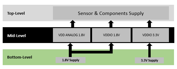
Two different power domains and one reference voltage are required for the Ganymed® system. On Top-Level the IO voltages are available to supply the sensors and peripherals.
Clocks
| Low power operation clock/boot clock | 32.768kHz |
| System reference clock | 25MHz |
| System clocks (internal) | Generated from external clock via PLL, as required for functional units |
| CPU clock | 400MHz maximum |
All clocks are integrated in the package. No external clock or oscillator is needed for the system. The CPU clock frequency can be set exclusively by the DAQU CPU core. All DPU cores operate at the same clock frequency (unless disabled), while the DAQU core frequency may be different.