
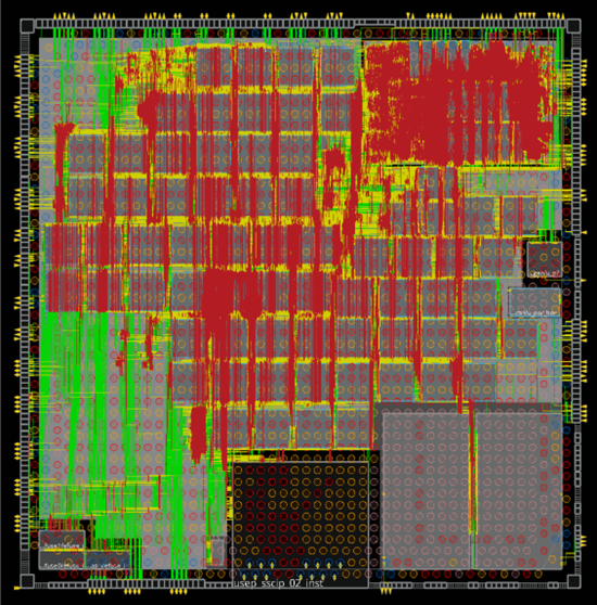
Ganymed-Core
Functional description
Overview
Revolutionized New Platform for All Integrated Smart & Secure Sensors
Next generation applications in logistics, robotics, automation, smart home and building, consumer and white goods, smart city and renewable energy require the adaption of smart and secure sensors with data connectivity. Existing semiconductor standard solutions often provide insufficient flexibility and missing software environment. The most critical item, however, is the missing inherent data security approach encompassing the complete value chain of the product.
The Solution
Sensry is a newly established company offers an smart edge sensor construction kit with highly flexible and customizable hardware configurations according to customer requirements. The universal sensor platform USeP combines cutting-edge assembly and packaging technologies with new design methods as well as various integration possibilities for sensors.
Features
- Multi-Core RISC-V performance for smart edge computing and AI applications
- Produced in Europe in latest Globalfoundries 22FDX technology
- Support of multiple communication standards
- Low power consumption
- Adequate memory resources
- Inherent multi-layer data security and authentication
- Software Ecosystem available
- Integration in fog, edge and cloud computing
- Optional integration support from Sensry
Key Features
- RISC-V Cluster Core
- Data acquisition Unit (DAQU) with FPU
- Single RI5CY Core (RV32IMFCXpulp)
- Base Integer Instruction Set
- Standard Extension for Compressed Instructions
- Integer Multiplication and Division Instruction Set Extension
- Single Precision Floating Point Extensions
- Special RI5CY extensions for Post-Incrementing load and stores, Multiply-Accumulate, ALU extensions and Hardware Loops
- Running at max. 400MHz
- Data Proc. Units (DPU) with FPU
- 8 RI5CY cores for parallel operation (8 x RV32IMFCXpulp)
- Included basic and advanced timers
- 256kB Tightly-Coupled Memory (TCDM)
- 512Byte instrucation cache for each core (4kB)
- Running at max. 400MHz each core
- Event bus
- DMA
- Data acquisition Unit (DAQU) with FPU
- Security features
- Life-Cycle & Run-Time Management
- Crypto Co-Processor
- Secure Boot ROM
- Secure MRAM / SRAM
- True Random Number Generator (TRNG)
- One-Time-Programmable Memory (OTP) for Keys and Certificates
- Interfaces
- 3x UART (up to 2Mbit/s, two of them with hardware handshake)
- 4x I2C (up to 400kHz)
- 4x I2S
- 7x SPI (up to 50MHz)
- CAN-FD
- RGMII with MDIO for Ethernet-Phy
- HyperBus (for external RAM/Flash)
- Debug JTAG | System JTAG
- 25MS/s 12bit High Speed SAR ADC
- 100kS/s 11bit Ultra Low Power SAR ADC
- 16Bit Sigma Delta ADC (Audio)
- 32 GPIO
- Each interface (except GPIO) can be induvidually disabled for power saving
- Memory
- 512kB Secure MRAM
- 512kB MRAM
- 64kB Secure SRAM
- 4MB SRAM
- Individual Data & Instruction Cache for DPU cores
Power
| Core Voltage | 0.8V |
| IO voltage | 1.8V and 3.3V |
| MRAM voltage reference | 0.6V |
| Analog Subsystem voltages | 0.8V and 1.8V |
| Maximum total power dissipation | < 1W |
Three different power domains and one reference voltage are required for the Ganymed® system.
Clocks
| Low power operation clock/boot clock | 32.768kHz |
| System reference clock(external oscillator) | 25MHz |
| System clocks (internal) | Generated from external clock via PLL, as required for functional units |
| CPU clock | 400MHz maximum |
The CPU clock frequency can be set exclusively by the DAQU CPU core. All DPU cores operate at the same clock frequency (unless disabled), while the DAQU core frequency may be different.
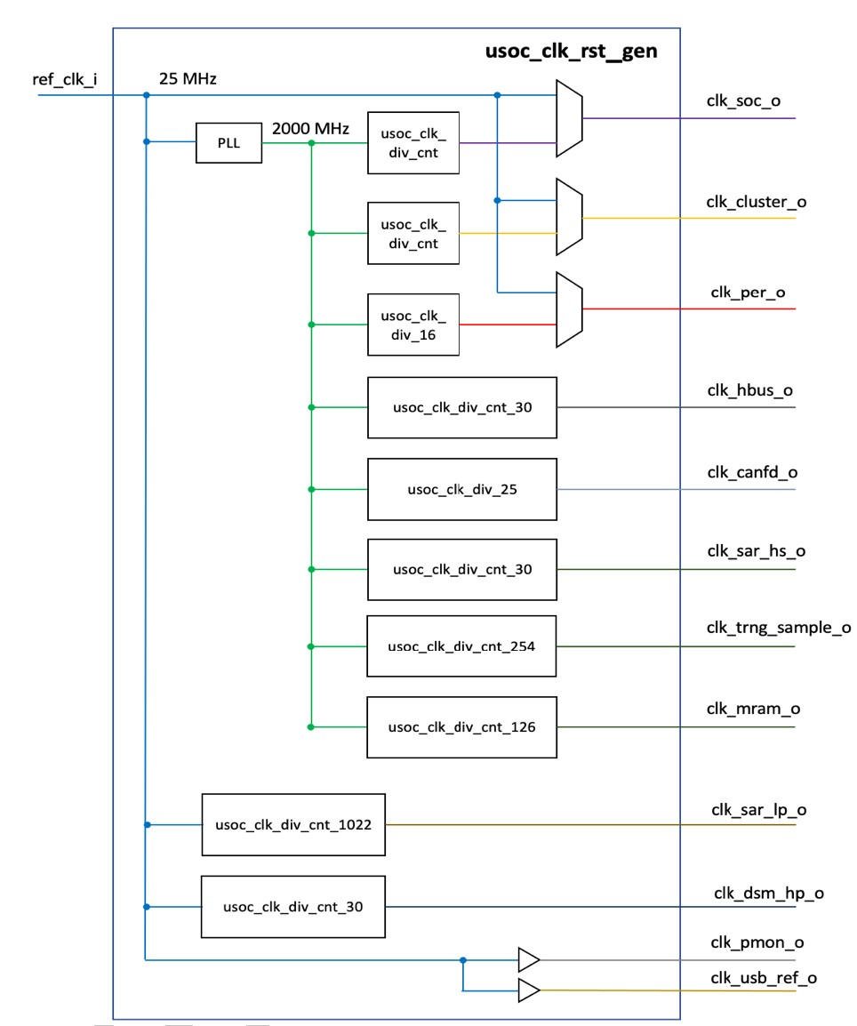
All the internal clocks are derived from a single PLL operating at a VCO clock source of 2 GHz generated from an extern reference clock of 25MHz. Most of the internal clock dividers are configurable. The DAQU and the peripheral logic can be multiplexed into the 25MHz reference clock domain to provide basic functionality if the PLL and clock dividers are uninitialized.
The following table describes the standard boot values for the clock divider:
| Clock Name | Brief Description | Default Reset Value |
|---|---|---|
| clk_soc_o | DAQU main SoC Clock | 100MHz |
| clk_cluster_o | DPU Clock | 100MHz |
| clk_per_o | Peripherals Clock (Including Ethernet) | 125MHz |
| clk_hbus_o | HyperBus Clock | 100MHz |
| clk_candfd_o | CAN-FD Clock | 80MHz |
| clk_sar_hs_o | High-Speed SAR ADC Clock | 500MHz |
| clk_trng_sample_o | CAN-TRNG sample Clock | 100MHz |
| clk_mram_o | MRAM Clock | 20MHz |
| clk_sar_lp_o | Ultralow-Power SAR ADC Clock | 2.5MHz |
| clk_dsm_hp_o | Delta Sigma ADC Clock | 12.5MHz |
| clk_pmon_o | Process Monitor Clock (not used) | - |
| clk_usb_ref_o | USB Ref. Clock (not used) | - |
Memory architecture
There are different types of volatile and non-volatile memories available on the Data Acquisition Unit (DAQU) and the Data Processing Unit (DPU) cluster. The different memories are accessible with different privileges in the memory map. External memory can be added via HyperBus interface in the Bottom-Level (PCB). Since the energy and performance cost of accessing external RAM over external buses is higher compared to the internal memory, generally this should be avoided as much as possible. In consequence, program code is loaded from external flash at boot into the DAQU SRAM.
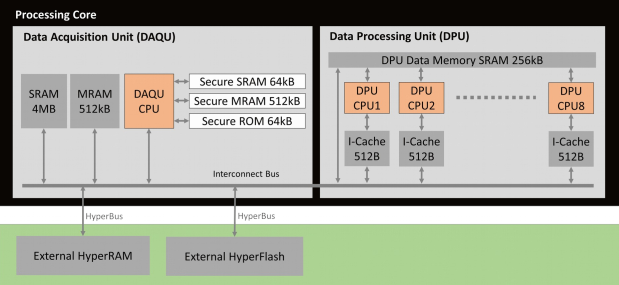
The secure memory part is not accessible from normal user mode privileges. All MRAM parts are FlashMRAM which means it has an internal flash memory interface. The Memory Map gives an overview over the address space.
| Name | Size | Start address | End address | Note |
|---|---|---|---|---|
| Global MRAM | 512KB | 0x1E00_0000 | 0x1E07_FFFF | |
| Secure MRAM | 512KB | 0x1D10_0000 | 0x1D13_FFFF | Secure Zone |
| Secure SRAM | 64kB | 0x1D02_0000 | 0x1D02_FFFF | Secure Zone |
| Secure Boot ROM | 64kB | 0x1D00_0000 | 0x1D00_FFFF | Secure Zone |
| SRAM CH0 | 32kB | 0x1C00_0000 | 0x1C00_7FFF | Only for DMA usage |
| SRAM CH1 | 32kB | 0x1C00_8000 | 0x1C00_FFFF | Only for DMA usage |
| Global SRAM | 4MB | 0x1C01_0000 | 0x1C20_FFFF | |
| DPU Data Memory SRAM | 256kB | 0x1000_0000 | 0x1003_FFFF | Tightly Coupled Memory |
Processing Layer
The processing core is based on the Open Source RISC-V instruction set architecture. The implementation consists of a Data Acquisition Unit (DAQU) which handles the wired and wireless communication, security features and memory and the Data Processing Unit (DPU) which consists of eight powerful RISCY processing cores with tightly coupled own memory and separate floating-point units. Additional several interfaces are integrated and distributed to the Top-Level and the BottomLevel. Figure 5 shows an overview of system interfaces and their connection to the different Levels.
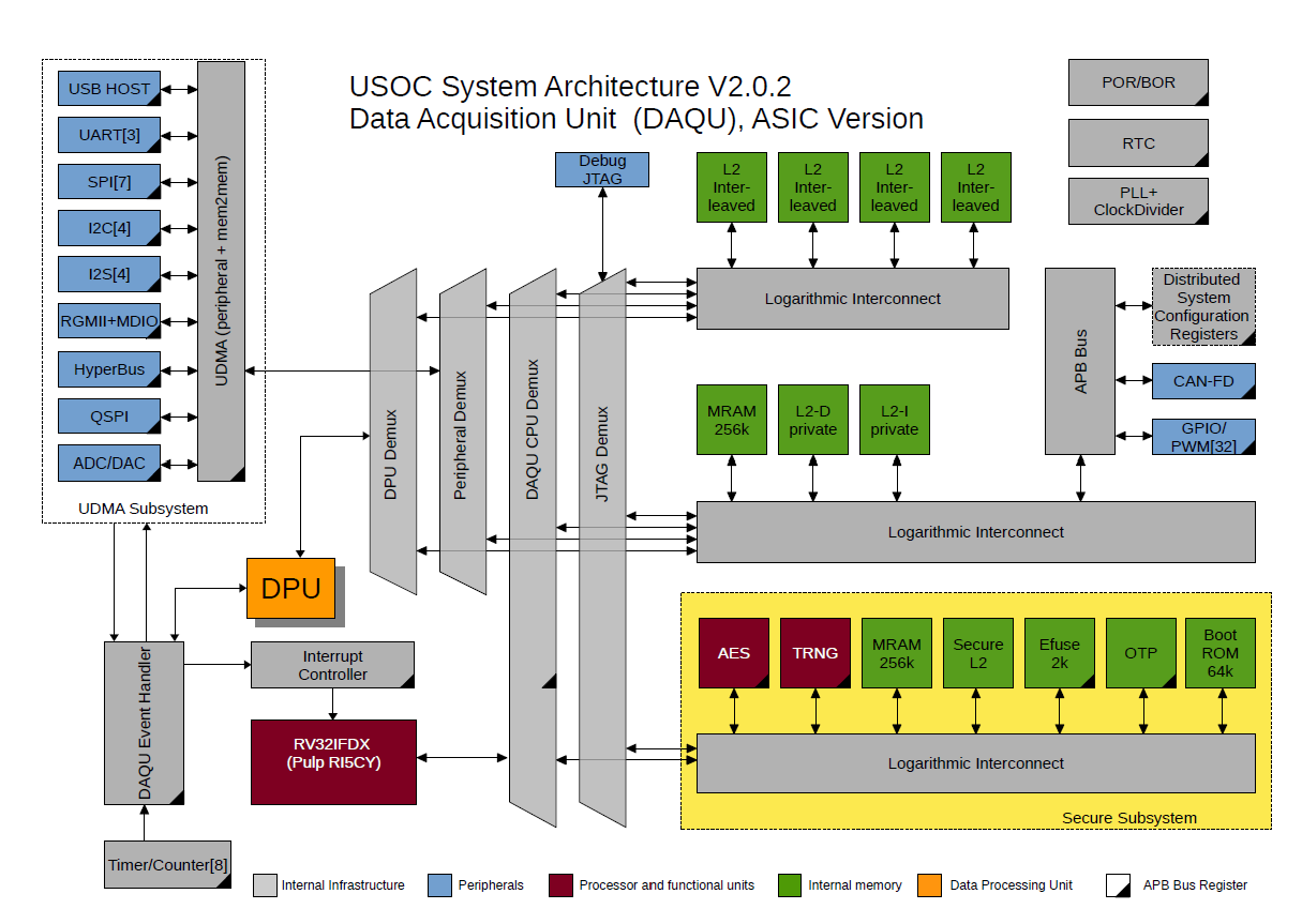
The processing core is divided basically into a data acquisition unit (DAQU) which controls the interfaces, main memory security subsystem (see Figure 4 for the DAQU schematic overview) and the data processing unit (DPU). The DPU is part of the heterogeneous multicore system and includes eight independent RISCY cores with tightly coupled memory and dedicated floating point units to enhance the system to high performance calculation platform. The DPU is designed to process sensors data independently to the main core and exchange data due to a direct memory access (DMA) controller. This allows to implement computationally intensive operations and data preprocessing needed for Edge and Fog Computing approaches.
Beside the standard interfaces like JTAG for programming and debugging, several serial interfaces, GPIOs and the HyperBus for HyperRAM and HyperFlash memory extension, the device includes a powerful analog interface to adapt raw analog sensors. This includes several analog-to-digital and digital-to-analog converter and their matching circuits. The RGMII interface implements a set of IEEE 802 Ethernet sub-standards in order to provide an ethernet time sensitive network (Ethernet TSN) interface. The automotive interface CAN is implemented regarding the latest standard ISO 11898-1 with flexible data rate (CAN-FD).
Reset Modes
Five reset modes are available. After reboot, the cause for the previous reset can be read from a status register during boot mode, except for power-on reset:
- Power on reset (POR)
- External reset from a reset input pin (XR)
- Software initiated reset (SOR)
- Brown-out reset (BOR)
- Watchdog reset by watchdog controller (WDR)
The watchdog reset can be issued by an internal watchdog controller.
Integrated Analog-Front-End
The core chip has three different analog-to-digital conversion blocks to allow the processing of a wide range of sensor signals. Each block can be shut down individually for optimized power consumption. A high speed 25MS/s SAR ADC with four parallel sampled inputs is used to convert the multiplexed analog signals with a resolution of 12 bit. It may be used to convert up to 4 parallel sensor signals with 3 MHz bandwidth in normal operation mode or in fast mode a 12 MHz analog signal at channel 0. For ultralow power applications a 100kS/s SAR ADC with 11bit resolution is available for the conversion of sensor signals up to 50kHz. Finally, a high resolution 16bit delta sigma ADC is provided for audio signals up to 16kHz, allowing audio applications like sound activation or speech recognition.
The analogue channels are controlled by the digital controller. Output data is provided to the digital part via a register bank. The three different conversion blocks can run in parallel.
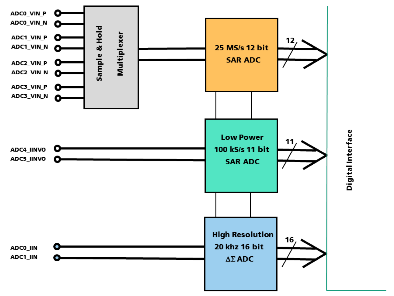
High Speed ADC Block
The fast 25 MS/s 12bit ADC is provided with a S&H stage which samples the four differential input signals x at the ADCx_VIN_P / ADCx_VIN_N interface (x=0 to 4) simultaneously. Then the sampled signal is multiplexed to the input of the 25 MS/s SAR ADC for conversion. After end of conversion, the 12bit output data is stored in a register to be read by the controller. This multichannel input block is intended for parallel sensors channels where a synchronous sampling is needed. The ADC run on a 500 MHz clock provided by the internal clocking block. However, in a fast mode the first of the four input channels can be selected permanently and an analog signal with a bandwidth up to 12,5MHz may be processed. All four input channels ADCx_VIN_P / ADCx_VIN_N interface (x=0 to 4) are specified for a differential input signal range of 0.4V +/- 0.3V, however they tolerate input signal levels from 0 to 0.8 Volt. Multichannel ultra sound or vibration sensors are one of the classes of sensors suitable for this block, due to its high frequency range. The digital result is provided in a 16bit frame – 12bit data, 2bit channel address, 2bit not used – to a FIFO register to be read by the controller on demand.
Ultralow Power ADC
An ultralow power SAR ADC with less than 40µA is implemented, to allow the conversion of sensor signals up to 50kHz bandwidth in battery operated mobile applications, e. g. for audio stand by and wake up modes. Sounds from the environment are monitored in an ultralow power standby listening mode and after activation the USOC is awakened to its full performance. Further applications may include standalone intrusion alarm or energy harvesting based early anomaly detection in machinery. The ADC is directly connected to the analog inputs ADC4_IINVO / ADC5_IINVO interface. The inputs are specified for a differential input signal range of 0.4V +/- 0.35V, however they tolerate input signal levels from 0 to 0.8 Volt. The maximum ADC sampling rate is specified with 100kS/s. The ADC can be operated in continuous conversion mode and in single shot operation mode. The conversion clock of 1.25 MHz is provided by the clocking block.
High resolution ADC
A 16bit Delta Sigma ADC is implemented for high resolution analog signal conversion. It may be used in combination with the low power ADC in audio and speech processing applications where the former is utilized in standby mode and after sound or command wakeup the DS-ADC provides a highresolution audio signal to the digital processor. The ADC is directly connected to the analog inputs ADC0_IIN / ADC1_IIN pads. The inputs are specified for a differential input signal range of 0.4V +/- 0.3V, however they tolerate input signal levels from 0 to 0.8 Volt. A block diagram of the ADC is shown in the following figure.
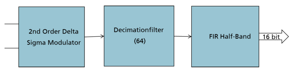
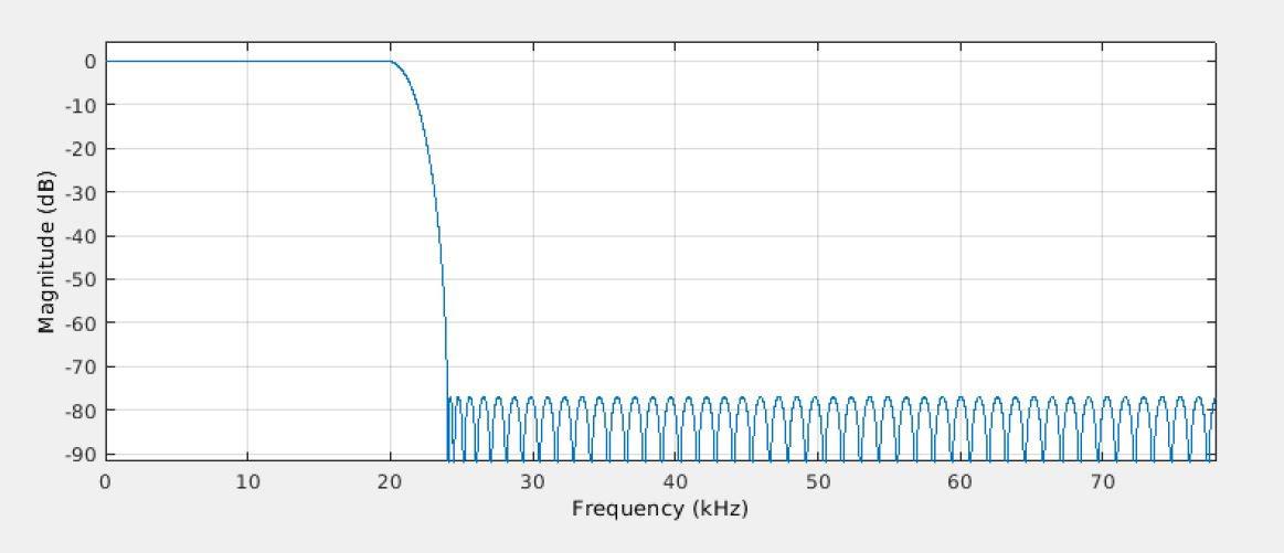
A 2nd Order Delta Sigma Modulator is followed by a 64-tap decimation filter and a FIR Half Band filter. The filter with an order of 120 is designed for a 20 kHz Bandwidth as shown in the following figure.
Security Subsystem
The security-relevant aspects of the universal sensor platform consist of four key areas: the device state, cryptographic functions, watchdog timers, and system boot:
- The device state defines device permissions and access restrictions. It ensures that secrets and features of the platform are always protected and only accessible from an appropriate system state.
- Cryptographic functions protect the platform and accelerate common cryptographic operations. They include functions for key management, cryptographic acceleration, and secure non-volatile storage.
- Watchdog timers increase the resiliency of the platform. With security-focused features, the watchdog timers protect devices from malicious software and support remote management.
- The system boot describes how the system is bootstrapped into a secure state. This includes verification of all software running on the platform.

Figure 11 shows an overview of the hardware part of the security subsystem from a functional perspective. The chip key and key control and status registers (CSRs) are designed to be compatible with the Trusted Computing Group (TCG) Device Identifier Composition Engine (DICE) architectures specification.
The device states
The device states regulate the access to privileged information in the system. The device state consists of two parts: the life cycle and the run-time state. The life cycle state is persistent on the device, the run-time state will be initialized with every reset. Both states together controls read and write access to memory locations and CSRs. The level of access to sensitive information is determined by the device state.
The life cycle states
In general, there are four different life-cycle states:
- Unlocked factory: initial state of all devices, active in factory
- Locked factory: intermediate state, active in factory
- Unlocked: initial state customers receive their devices in, active during development and at customers factory
- Locked: final state, active in field
The allowed transition between the states is shown in Figure 12.

The run-time states
The run-time state primarily controls access to the chip key via the machine mode key (mkey). It is used by software, in its secondary function, to determine software access permissions. The Run-time state consists of four different states: evaluate, secure, non-secure, and security violation. It is a dynamic state, which is reevaluated at every reset.
- Evaluate: The initial state after every reset is the evaluate state. It is an intermediate state only active during the secure boot process. The mkey CSR is reloaded with the reset value.
- Secure: The secure state is entered if the secure boot process has been successfully completed. The mkey CSR is reloaded with the chip key on state entry. Software has read and write access to the CSR and may use it for cryptographic operations.
- Non-Secure: In the unlocked factory and unlocked life cycle states, the nonsecure state is entered if unsigned software is running on the device. In the locked factory and locked life cycle states, the nonsecure state may be entered by software running in the secure runtime state.
- Security Violation: The security violation state is entered to protect the system on errors. The mkey CSR is zeroized on entry to prevent software from accessing it. Keys derived from it and data protected with it are inaccessible.

Figure 13 shows the transition scheme between the four different states. The transit from one state to another, security conditions have to be fulfilled.
Cryptographic functions
Cryptographic functions provided by the platform are divided into four categories: key management, device identification, accelerators, and secure non-volatile memory. They are summarized below:
- Key management
- Chip key
- Key CSRs
- Certificate slots
- Device identification
- Cryptographic accelerators
- AES (128,192,256)
- SHA256
- True Random Number Generator (TRNG)
- Secure Non-Volatile Storage
Key management consists of two parts, the chip key in combination with the key CSRs and certificate slots. Key CSRs are used on the platform to store and use cryptographic keys. The mkey CSR makes the chip key — a device-unique key — available to machine mode software. The user mode key (ukey) CSR is an optional key CSR available to user mode software. Certificate slots are used on the platform to store certificates for secure boot and secondary purposes. The platform has two certificate slots, one for Universal Sensor Platform and customer certificates each.
The platform provides a set of cryptographic accelerators, listed above. They are only available to the main processor. Additionally, the system provide dedicated non-volatile storage for security-critical information, including cryptographic keys, configuration data, and software states. It is only accessible to machine mode software, but parts of it may be made available to user mode software through an Application Programming Interface (API).
Security-enhanced Watchdog timers
A conventional watchdog timer consists of a timer with a software-configurable timeout interval. Once started, software can defer the watchdog timer to reset it to the specified timeout value. If the timer elapses and is not deferred, the device is reset by the watchdog timer.
The security-enhanced watchdog timer extends the conventional watchdog timer with a set of new requirements. Each requirement may be set to enforcing by software. However, the watchdog timer is only considered to be a security-enhanced watchdog timer if all requirements are set to enforcing.
System Boot
The system boot process securely starts and initializes the Universal Sensor Platform. This process is performed by ROM software, which is the first software to run after a reset. It performs the necessary steps to load and verify software images on the platform as part of secure boot.
Secure boot uses certificates verify software and data. The secure boot mode configuration determines how the certificate chain is used in the secure boot process. It must be set during manufacturing by configuring the relevant entry in OTP memory. There are two modes, CA mode (optionally with enforce CA signature configuration) and legacy mode.
The following describes the individual steps of the secure boot process. All steps of the process are implemented in ROM software. A security violation is raised if an error occurs at any part of the secure boot process:
- System Initialization: The Main processor core is the first processor to start after areset. It runs from the on-chip ROM and contains the secure boot firmware. It performs all necessary system initialization steps before continuing to the software image search step.
- Software Image Search: In the software image search step, all software sources are searched in the system boot order for valid software images. This includes flash storage, for example connected to the quad-SPI interface, but also communication interfaces such as UART. The latter may be used for development or recovery purposes, where there are no valid software images available locally. The software image is transferred into main processor memory, from where it is verified as part of the following steps.
- Certificate Chain Verification: The certificates entry in the software image is verified in four steps, listed below. Certificates are installed for software verification in the next step, if the verification passes.
- Verify format of root certificates (including number of expected certificates)
- Verify certificates against hashed copy in certificate slots
- Verify certificate chain
- Verify certificate serial numbers (if required)
- Software Verification: Software in the software blobs is verified using the type A certificates installed in the previous step. If software for the main processor is encrypted, it is decrypted after verification. Software is then started in the normal operation step. In the locked factory and locked device life cycle states, all software included in the software image must be signed. A security violation is raised if this is not the case. In the unlocked factory and unlocked device life cycle states, not all software must be signed. The unlocked factory state, in specific, requires no signed software; the unlocked state requires software to be signed.
Software Eco System
The Software Eco System consists of three parts:
- Development system including built tools and development environment
- Application programming interfaces (APIs) in form of libraries to control different system parts
- Client-side tools and example implementations
Generally, the embedded software is running as a Real-Time-OS (RTOS) implementation which divides in a Machine-Mode and User-Mode (comparable to Kernel- and User-Mode on Linux based Systems). The two modes allow a different level of access to critical parts of the system. Figure 14 shows the general functionality of the API system.
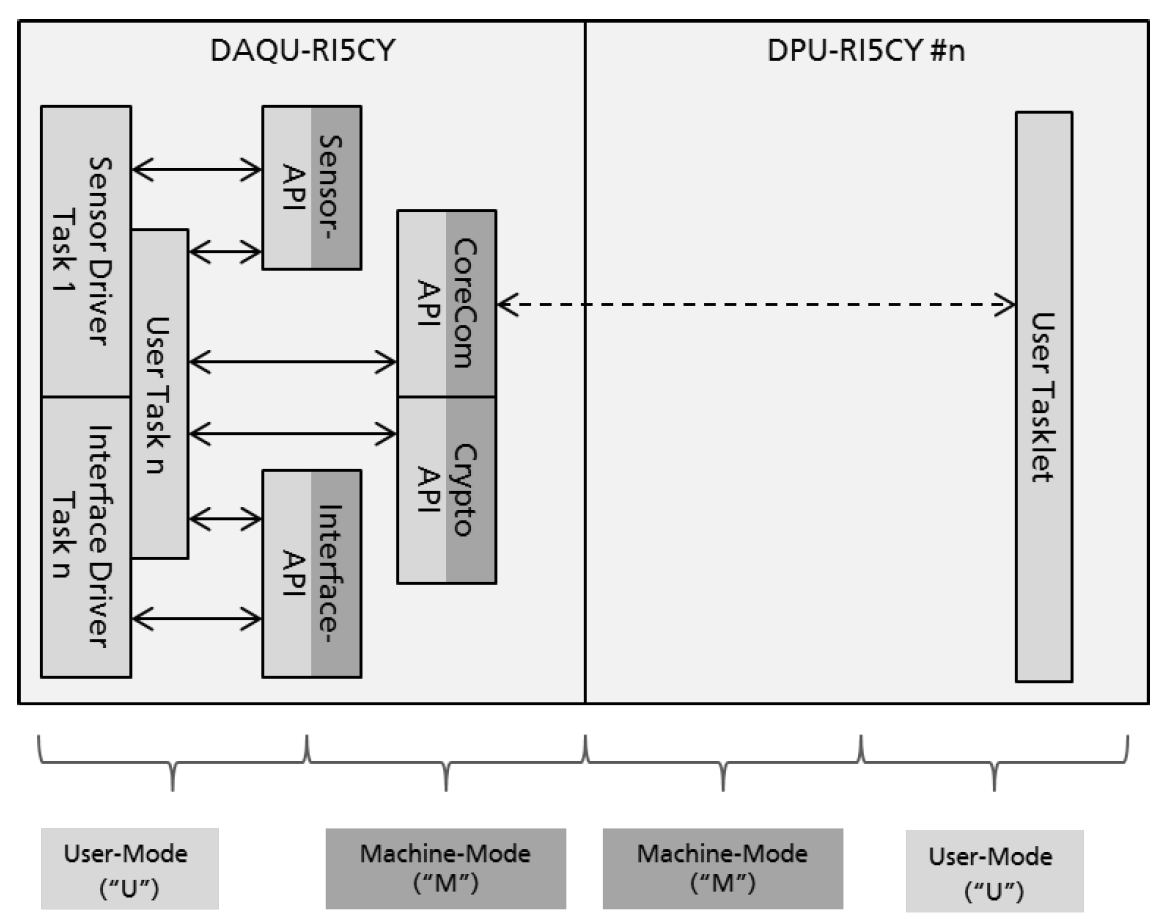
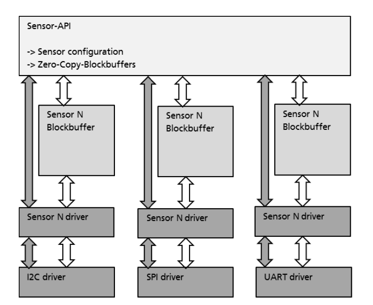
The Sensor API controls the low-level communication and data transfer between the sensor and the system. An overview of the Sensor API is shown in Figure 15.
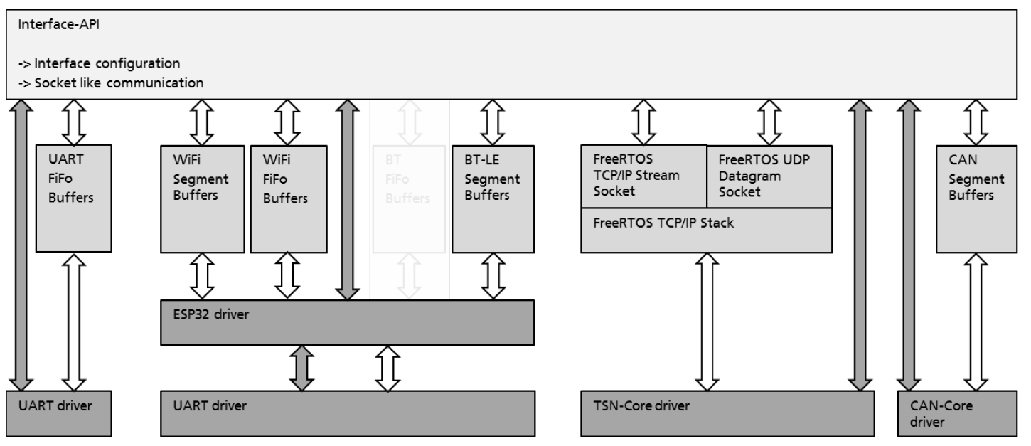
The Interface-API provides a socket-based communication to all interfaces. An overview of the Interface-API is show in Figure 16.
The CoreCom-API controls all operating system relevant features including management of the DPU cluster. This API initiate and controls “Tasklets” running independently on one of the DPU cores. The Security-API interfaces between the hardware security features and software.
Manufacturing Process
The system in package (Top- and Mid-Level) will be manufactured in the supply chain of Sensry. The Bottom-Level can be manufactured by costumer or system integration partner of Sensry. The possible workflow is shown in Figure 2.

The device contains a strong security concept which allows to set-up trustful and reliable sensor data driven business models. The hardware integrated security core includes a secure one-timeprogrammable memory model for the device states, keys and certificates as well as cryptographic functions, security watchdog timer and a secure system boot process. The costumer deployed software must interact with these security features in order to fulfill the desired security standard. The security concept itself is explained in a different chapter.